Introduction: Small Devices, Giant Impact
In a world increasingly shaped by technological precision, few fields are as quietly revolutionary as the science of microdevices. These devices have functional elements measured in micrometers — about the width of a human hair. The foundation of modern microdevices was laid in 1959, when physicist Richard Feynman delivered his landmark lecture “There’s Plenty of Room at the Bottom” at Caltech, USA, inspiring decades of miniaturization research. The first practical MEMS (Micro-Electro-Mechanical Systems) device, a microscopic pressure sensor, was developed in the early 1960s at Stanford University, California. By 1987, Texas Instruments (USA) had pioneered the Digital Micromirror Device (DMD), a breakthrough in microdevice applications. Despite their tiny size, they are used in space exploration, biomedical diagnostics, industrial sensing, telecommunications, and consumer electronics. Bosch (Germany) began mass-producing MEMS sensors in 1995, making them a staple in smartphones and automotive systems. STMicroelectronics (Switzerland/Italy) and Qualcomm (USA) further advanced microdevices for satellites and consumer electronics throughout the 2000s. Advanced biosensors capable of detecting diseases before symptoms appear were significantly advanced by companies like Abbott Laboratories (USA) and Roche (Switzerland) in the 2010s.
Microdevices sit at the intersection of engineering, physics, chemistry, and biology. The field gained major institutional momentum with the establishment of dedicated MEMS research centers worldwide, including IMEC in Belgium (founded 1984) and DARPA-funded programs in the USA throughout the 1990s and 2000s. Understanding them means understanding one of the most consequential frontiers in modern science and technology.
What Are Microdevices?
A microdevice is any device whose critical functional elements operate at the microscale typically between 1 and 500 micrometers (μm). To put this in perspective, a single human hair is approximately 100 μm wide. At this scale, conventional manufacturing techniques give way to specialized processes borrowed from the semiconductor industry, such as photolithography, electron-beam lithography, and chemical vapor deposition.
Microdevices differ from nanodevices in that they intentionally target this intermediate scale rather than pushing toward atomic dimensions. While the global semiconductor race drove engineering toward sub-10nm transistors, the microscale was often bypassed yet it holds enormous untapped potential. Researchers at institutions like Whitworth University’s Microdevices Laboratory are now deliberately returning to this scale to explore applications that were skipped over during the nanoscale race.
The categories of microdevices are broad and include microelectromechanical systems (MEMS), microfluidic devices, photonic microdevices, sensing devices, crystal devices, and more each serving distinct purposes across industries.
The Science Behind Microdevices: Core Technologies
Crystal Technology
One of the most foundational technologies in microdevices is the use of quartz crystals. Epson, a global leader in microdevice manufacturing, has built much of its microdevice portfolio around crystal expertise. Engineers and device makers prize quartz crystals for their exceptional frequency stability, low power consumption, and resistance to environmental noise. They form the backbone of crystal units, crystal oscillators, and real-time clock (RTC) modules components critical to keeping time, maintaining wireless communication frequencies, and synchronizing electronic systems.
Epson’s crystal devices serve markets including 5G telecommunications, IoT (Internet of Things), and automotive applications where timing precision is non-negotiable. In a 5G base station, for example, even a fractional frequency deviation can disrupt data transmission across thousands of connected devices.
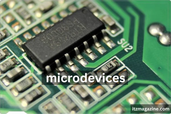
Semiconductor Microdevices
Semiconductors represent the computational heart of modern microdevices. At Epson, extremely low power consumption and LCD driver technologies are core hallmarks of their semiconductor line, which includes ASICs (Application-Specific Integrated Circuits), MCUs (Microcontroller Units), LCD controllers, and voice guidance ICs.
Low-power semiconductors are essential, not optional. They power IoT devices and wearable electronics where batteries must last months or even years. Seiko Epson Corporation combines crystal and semiconductor technologies to create highly integrated, energy-efficient solutions. These innovations enable compact devices to perform at higher levels.
MEMS: Micro-Electromechanical Systems
MEMS devices are miniaturized structures that combine mechanical and electrical components on a single chip. They are perhaps the most versatile class of microdevices, appearing in airbag sensors in automobiles, gyroscopes in smartphones, pressure sensors in medical equipment, and microphones in hearing aids.
NASA’s Jet Propulsion Laboratory (JPL) Microdevices Laboratory (MDL) has been a major pioneer in MEMS research, developing nanofabrication techniques that push MEMS to operate in the extreme conditions of space vacuum, radiation, cryogenic temperatures, and prolonged mission durations. Their work demonstrates that microdevices are not just a commercial technology; they are mission-critical infrastructure for scientific discovery.
Sensing Devices: Microdevices That Perceive the World
Among the most impactful microdevices are those designed to sense physical phenomena with extraordinary precision. Epson’s sensing division, for example, produces accelerometers, vibration sensors, gyro sensors, and inertial measurement units (IMUs) all based on quartz crystal technology.
These sensors exploit the piezoelectric properties of quartz: when the crystal is mechanically stressed, it generates an electric charge. This charge can be measured and converted into data about motion, vibration, orientation, or acceleration.
Gyro sensors from Epson are used in digital cameras to stabilize images compensating for hand tremors so that photographs remain sharp even in motion. The same principle is applied to autonomous guided vehicles (AGVs) in warehouses and factories, where precise navigation requires continuous measurement of angular velocity.
IMUs (Inertial Measurement Units) combine gyroscopes and accelerometers to provide full six-degrees-of-freedom motion tracking. Applications include autonomous vehicle navigation, aircraft attitude control, drone stabilization, and even earthquake monitoring in civil infrastructure.
Vibration and acceleration sensors are being deployed in structural health monitoring embedded in bridges, buildings, and industrial machinery to detect anomalies before they become catastrophic failures. This is the quiet promise of microdevices: turning invisible physical signals into lifesaving data.
Microdevices in Space: NASA’s Microdevices Laboratory
One of the most remarkable applications of microdevice technology is in space exploration. NASA’s Jet Propulsion Laboratory (JPL) hosts one of the world’s most advanced microdevice research centers: the Microdevices Laboratory (MDL) in Pasadena, California.
The MDL’s mission is to develop micro and nano-fabrication techniques that enable JPL and NASA to carry out new missions and perform measurements previously thought impossible. Their core competencies span an impressive range:
Mid-Infrared Detectors: These allow scientists to observe the planet Earth in specific infrared regions, map ecosystems, monitor cloud structures, and detect natural disasters. The same technology supports defense applications and atmospheric research.
UV-Visible Detectors and Systems: MDL advances in this area extend humanity’s vision to unprecedented sensitivity, enabling the detection of faint astronomical objects and fine atmospheric particles.
Submillimeter and Terahertz Devices: Researchers at MDL specialize in submillimeter-wave and terahertz remote sensing, technologies that penetrate materials that block visible light and can reveal hidden structures in both space and Earth observation.
Superconducting Devices: MDL develops superconducting nanowire single-photon detectors (SNSPDs), which are so sensitive they can detect individual photons of light. These devices were used in NASA’s Deep Space Optical Communications (DSOC) experiment demonstrating laser communication from deep space for the first time.
Semiconductor Lasers: Over two decades of refinement have produced semiconductor lasers that operate above room temperature with high output power and low energy consumption. Tunable laser spectrometers (TLS) use these lasers to measure gas abundances and isotope ratios in Earth’s and Mars’ atmospheres.
Diffractive Optics: Using electron-beam lithography, MDL fabricates unique nanostructures and optical elements that enable spacecraft instruments to perform novel measurements, including mapping light from the very first stars formed in the early universe.
Chemical Analysis and Life Detection: MDL designs in-situ instruments to search for signs of past or present life on Mars, making it perhaps the most scientifically thrilling application. Miniaturized mass spectrometers and chemical analyzers fly aboard planetary landers, analyzing soil and atmospheric samples millions of kilometers away.
The MDL embodies the philosophy that big things truly come from small technologies.
Biomedical Microdevices: Engineering at the Scale of Life
Nowhere is the promise of microdevices more personal than in biomedical engineering. At Michigan Technological University (MTU), the Biomedical Engineering department runs a dedicated Microdevices research group focused on engineering solutions to medical challenges at the microscale.
Biomedical microdevices bridge engineering and medicine, creating tools that interact with biological systems at the cellular and molecular level. Key research areas include:
Lab-on-a-Chip Systems: These devices miniaturize an entire laboratory’s worth of diagnostic capability onto a chip the size of a credit card. They can perform blood analysis, detect pathogens, measure biomarkers for disease, and sequence DNA all from a tiny sample and in a fraction of the time of traditional lab methods. Whitworth University’s Microdevices Lab has developed lab-on-a-chip technologies specifically for disease detection, leading to the launch of Pacific Microdevices the first spin-off company in Whitworth’s history in 2025.
Biosensors — Microscale biosensors can detect biological signals from glucose levels in blood to the presence of cancer biomarkers — with extraordinary sensitivity and specificity. By integrating biological recognition elements (like antibodies or enzymes) with electronic transducers, these sensors convert biological events into measurable electrical signals.
Microfluidic Devices: These are systems with fluid channels on the micron scale, capable of precisely controlling tiny volumes of liquids. Applications include cell sorting, drug delivery systems, point-of-care diagnostics, and even the study of living organisms in controlled microscale environments. Researchers at Whitworth’s Microdevices Lab have demonstrated the use of microfluidic channels as narrow as 200 μm to analyze C. elegans a microscopic worm widely used as a model organism in biological research with fluorescent imaging of internal structures.
Implantable Microdevices: The future of personalized medicine includes microdevices implanted within the human body to continuously monitor physiological parameters, deliver drugs on demand, or stimulate neural tissue to treat neurological disorders. These devices must be biocompatible, miniaturized, low-power, and capable of wireless communication demands that push every branch of microdevice engineering to its limits.
Photonic Microdevices: Controlling Light at the Microscale
Photonics the science of generating, controlling, and detecting photons (light particles) is one of the most exciting frontiers of microdevice research. Photonic microdevices manipulate light to interact with matter, enabling applications in telecommunications, sensing, computing, and biomedical imaging.
At Whitworth University’s Microdevices Lab, photonic research centers on waveguides essentially pipes for light that direct photons to areas of interest. A ridge waveguide, for example, may be just 30 μm wide and 5 μm high, yet it can guide light with remarkable efficiency. These waveguides are fundamental components of integrated photonic circuits the optical equivalent of electronic integrated circuits that form the backbone of fiber-optic telecommunications networks and on-chip biosensors.
Photonic microdevices offer critical advantages over purely electronic devices light travels faster than electrons, generates less heat, and can carry vastly more information in parallel through different wavelengths (wavelength division multiplexing). As data demands continue to explode, photonic microdevices may be the key to sustaining the speed and capacity of global communications infrastructure.
At NASA’s MDL, photonic microdevices have enabled breakthrough capabilities in space from detecting the faint infrared signatures of distant galaxies to measuring the isotopic composition of Martian soil with laser spectrometers.
Manufacturing Microdevices: The Fabrication Revolution
Creating devices at the microscale requires extraordinary manufacturing precision. The field of microfabrication draws heavily from the semiconductor industry, employing techniques such as:
Photolithography: Using ultraviolet light and photosensitive materials to pattern structures on a substrate with submicron precision. Manufacturers use the same process for computer chips and adapt it for microdevice production.
Electron-Beam Lithography: A more precise (but slower) technique using focused electron beams to write patterns at nanometer resolution. NASA’s MDL uses this to fabricate unique nanostructures for diffractive optics.
Soft Lithography and 3D Printing: Emerging methods that use flexible molds or additive manufacturing to create microfluidic channels and microdevice structures more affordably. Whitworth’s Microdevices Lab has developed 3D-printed PCR devices—compact systems for DNA amplification that could transform field diagnostics.
Chemical Vapor Deposition (CVD) and Etching: Techniques for depositing thin films of material onto substrates and selectively removing material to create precise three-dimensional structures.
The convergence of these manufacturing methods with advanced materials including silicon, gallium arsenide, lithium niobate, and various polymers continues to expand what is possible at the microscale.
Microdevices and the 5G/IoT Revolution
The deployment of 5G networks and the explosive growth of IoT devices have made microdevices more strategically important than ever. Every wireless sensor, smart device, autonomous vehicle, and industrial machine relies on microdevices for precise timing, sensing, and efficient computation.
Crystal oscillators in 5G base stations must maintain frequency accuracy to within parts per billion. MEMS sensors in IoT nodes must consume microwatts of power while operating for years without maintenance. Microcontrollers must process sensor data locally (edge computing) to reduce latency and bandwidth demands on network infrastructure.
Epson combines crystal, semiconductor, and sensing technologies in one integrated approach. This positions the company as a key supplier for the 5G and IoT ecosystem. Billions of products worldwide use its microdevices. Most operate behind the scenes. They help connected systems run with high precision and reliability.
Challenges and the Road Ahead
Despite remarkable progress, microdevice engineering faces significant challenges:
Packaging and Integration: Getting microscale devices into real-world products requires packaging that protects them from environmental stresses while maintaining their performance. This remains a major engineering bottleneck.
Power Supply: Many microdevices, particularly implantable biomedical devices and remote IoT sensors, must operate on minimal power for extended periods. Energy harvesting from vibration, heat, or light at the microscale is an active area of research.
Biocompatibility: For medical microdevices, ensuring that materials and coatings do not trigger immune responses or degrade inside the body is a critical and unsolved challenge.
Scalable Manufacturing: Researchers must translate laboratory demonstrations into reproducible, high-yield manufacturing processes. The path from proof-of-concept to mass production is often long and expensive.
Regulatory Approval: Medical microdevices must navigate complex regulatory frameworks (such as FDA approval in the United States) before reaching patients a process that can take years.
Yet the momentum is undeniable. Academic labs are launching startups like Whitworth’s Pacific Microdevices. National labs are advancing measurement science. Major corporations are investing billions in microdevice technologies.
Conclusion: A Small World With Enormous Possibilities
Microdevices occupy a unique position in the technological landscape. Too small to see with the naked eye, yet large enough in impact to reshape medicine, exploration, communication, and environmental monitoring. They represent the quiet precision underlying the most visible technologies of our time.
From Epson’s crystal oscillators keeping 5G networks synchronized, to NASA’s superconducting photon detectors exploring the universe, microdevices power modern technology. Lab-on-a-chip systems may soon detect cancer from a single drop of blood. These tiny devices are the invisible engines of progress.
As researchers advance fabrication, materials science, and integration, microscale technologies will unlock innovations we can barely imagine. The future, it turns out, is very small and very powerful.